Management and Application of Power Supply

Copyright Notice:
This article is licensed under CC BY-NC-SA 4.0.
Licensing Info:
- Title: Loop Analysis - With Example of TIA
- Author: EleCannonic
- Link: https://elecannonic.com/categories/electronics/power/
Commercial use of this content is strictly prohibited. For more details on licensing policy, please visit the About page.
Power Supply is the most important component in all electric systems. Generally, in one system there’ll be multiple supplies. For example in an ADC an analog voltage 5V and a digital supply 3.3V might be required. The most widely used topologies are DC-DC converter (buck-boost) and low dropout regulator (LDO).
1. Buck Converter
Buck is used to generate a lower voltage supply.
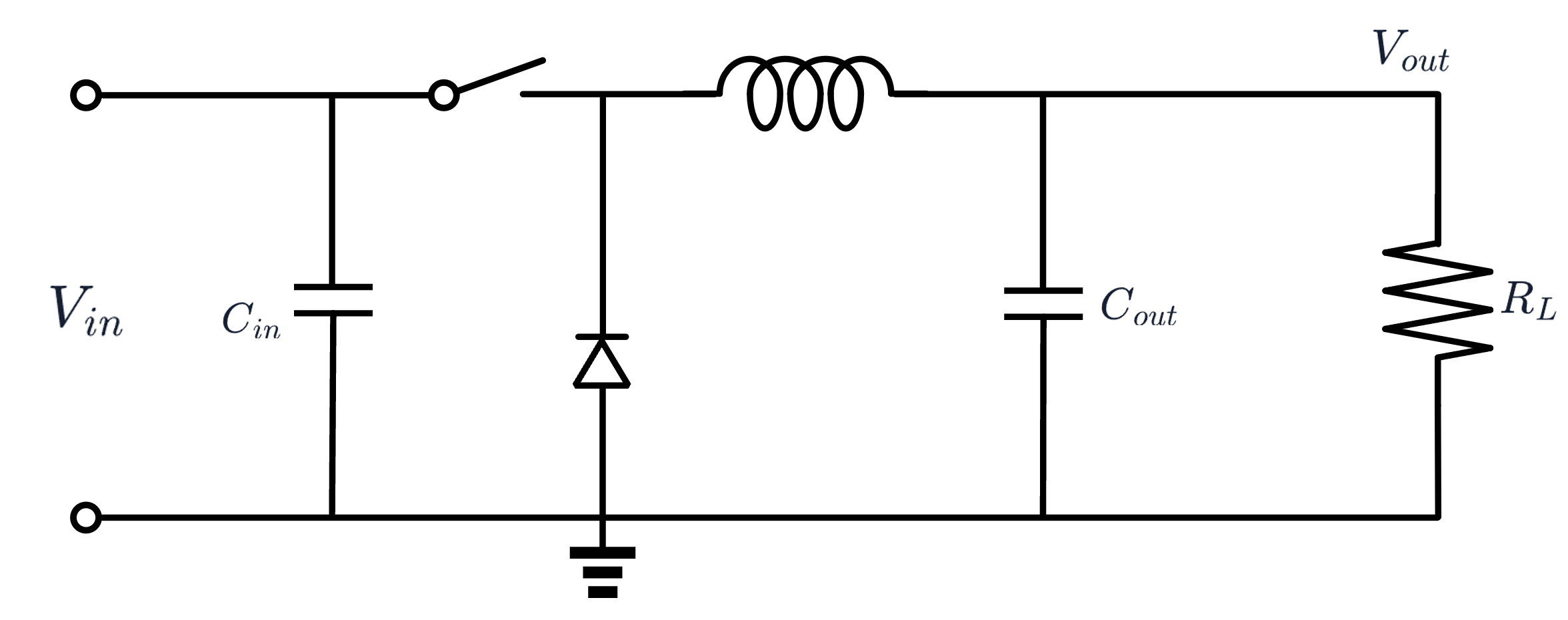
When the switch is on,
When the switch is on,
and when the switch is off,
If we turn on and off the switch at a certain frequency with a duty ratio of
Combine and solve:
Since
Next, let’s analyze the operating phases. During
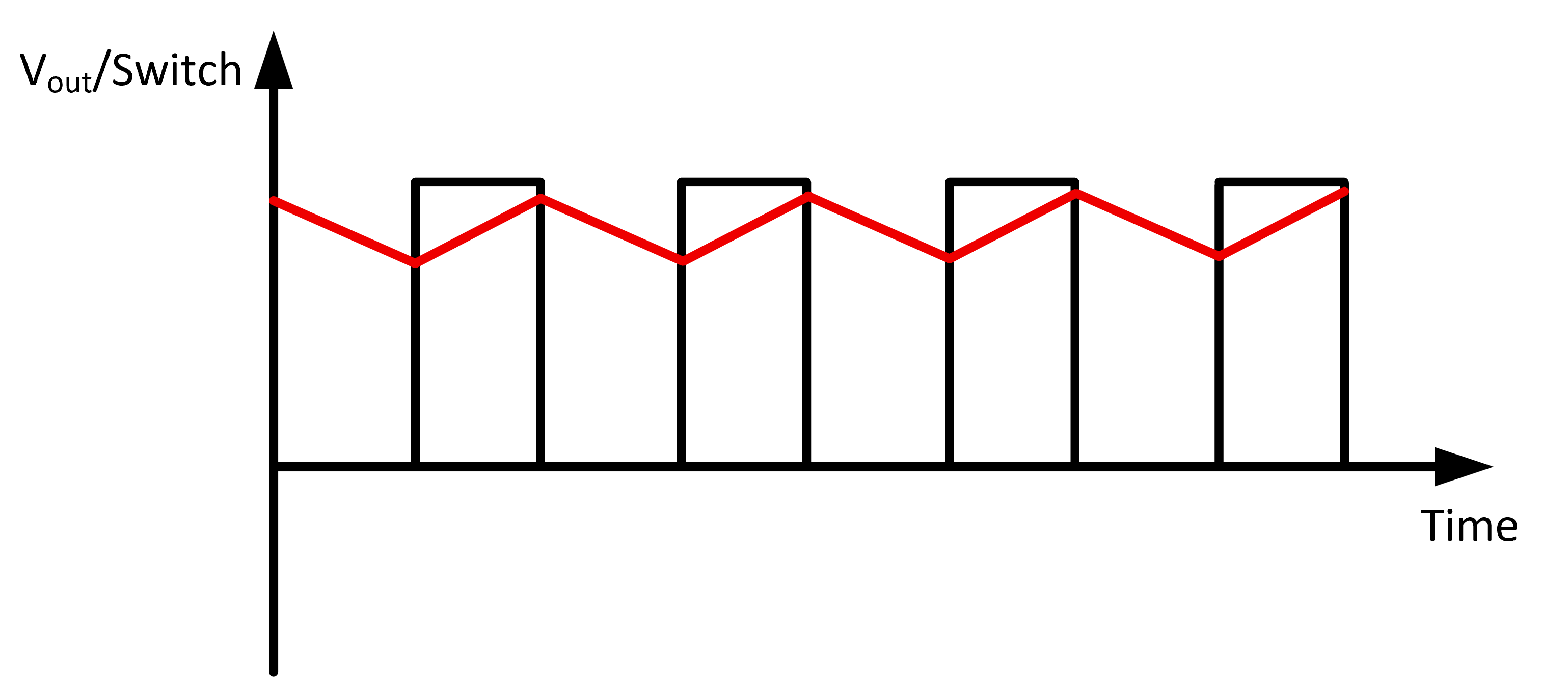
On the oscilloscope you can see some unexpected AC components, whose frequency is approximately the same as the switching frequency. This AC component is called ripple. Ripple is a primary drawback of the Buck converter (and the Boost in the following section). Clearly, faster switching produces ripple with smaller amplitude but higher frequency, while slower switching produces ripple with lower frequency but larger amplitude.
Another significant drawback is the electromagnetic interference (EMI). During
According to Faraday’s law of induction, an electromotive force (EMF) is induced across the parasitic inductances by this fast-varying current:
If the hot loop has a large physical area, the parasitic inductance within the traces acts as a loop antenna, generating strong radiated magnetic fields and severe high-frequency voltage ringing at the switching node. To effectively suppress this EMI at the source,
From the perspective of power efficiency, the main energy dissipation of a buck converter is dominated by conduction losses due to the parasitic resistances of the components (like the inductor’s DC resistance and PCB trace resistance) and switching losses incurred during the turn-on and turn-off transitions. Because these parasitic losses are relatively low compared to the total throughput, the efficiency of a practical Buck converter can easily reach approximately 90%.
2. Boost Converter
Unlike a buck converter, a boost converter can only be used to increase the voltage.
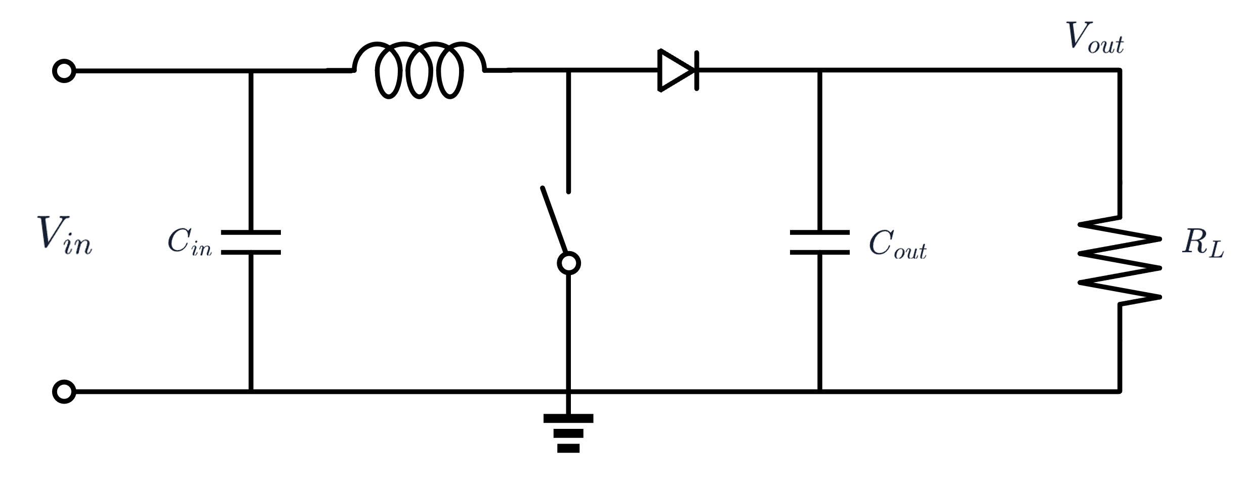
Similarly, during
During
Solve
Similarly to the buck converter, a boost converter also suffers from ripple and EMI. In the boost circuit, the loop
If you need a negative voltage but your input is a single positive one, you need the buck-boost.
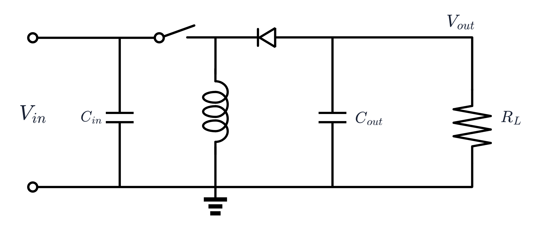
You can easily recognize the input and output loops. In the input loop
In the output loop
Solve
You still failed to escape from the disturbance of ripple and EMI.
3. Application with MOS
In most integrated DC-DC converter the switch and diode are both replaced with MOSFETs. Another control logic applies PWM waves on the gates of the two MOS’s. Generally, the MOS replacing the switch is called “high-side MOSFET”, while the one replacing the diode is called “low-side MOSFET”.
A combined circuit is displayed below
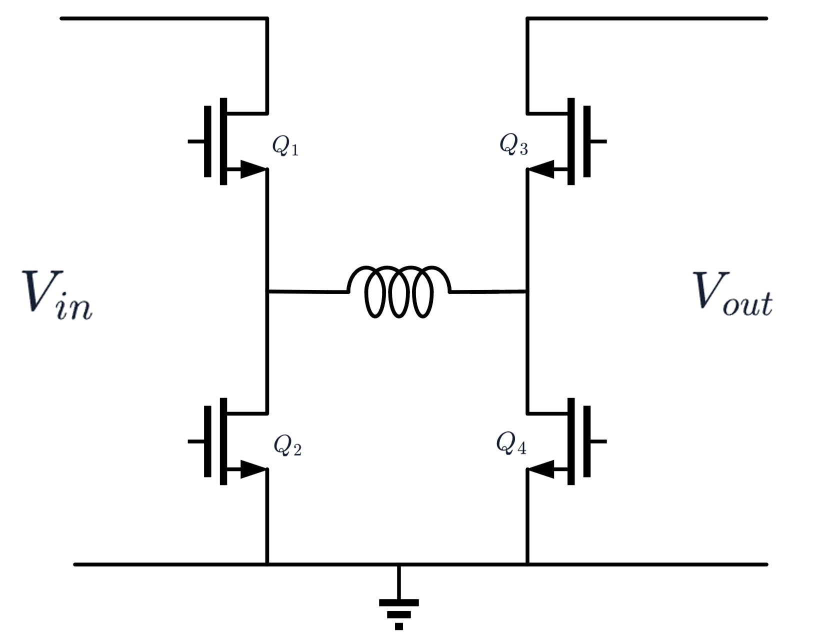
Conduct Q1 and cut Q2, Q3 serves as the switch and Q4 serves as the diode, the circuit serves as a boost. And when Q3 on, Q4 off, it becomes a buck. The chips sold on the market (buck or boost only) contains only two of the MOS’s.
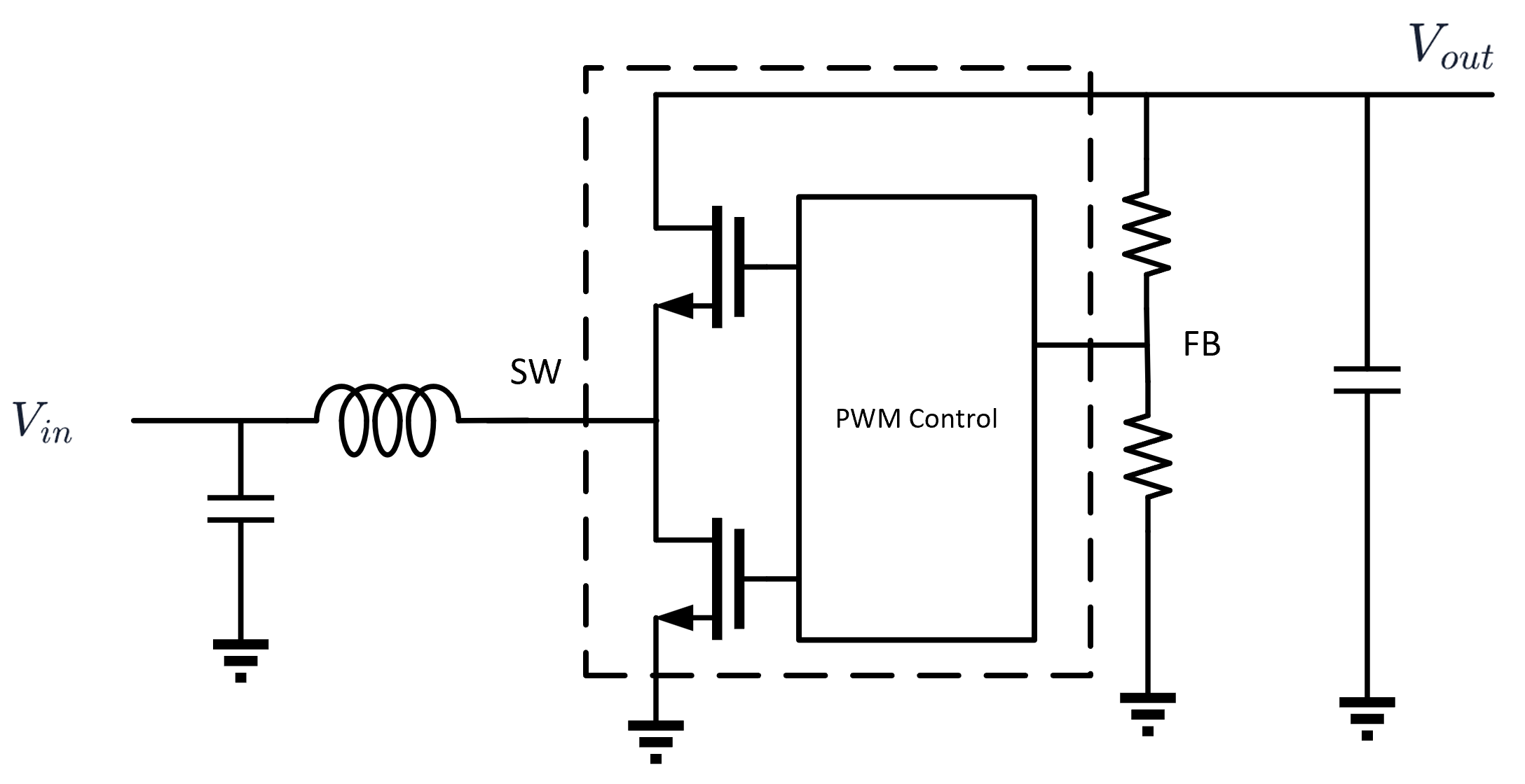
Two critical pins are designated as SW (Switching Node) and FB (Feedback) respectively. The SW pin denotes the power node between the high-side and low-side MOSFETs, where the external power inductor must be connected. The FB pin connects back to the internal control logic module to monitor the real-time output voltage. In most buck and boost converters, an integrated control module automatically regulates the switching frequency and duty ratio based on this feedback signal to maintain a stable output.
A typical example is TPS54302, a buck converter developed by TI. In the datasheet, TI has provided a well-designed application schematic.
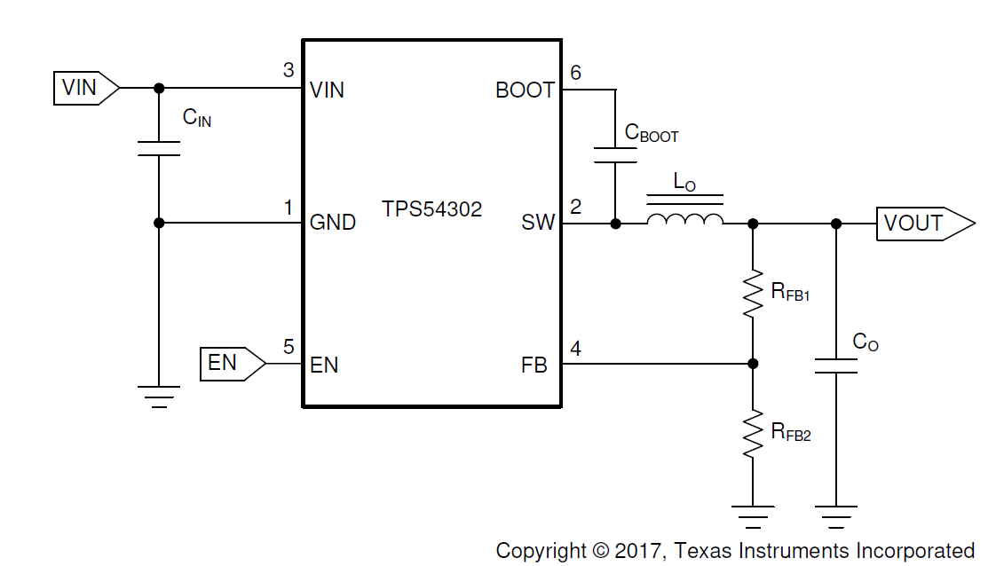
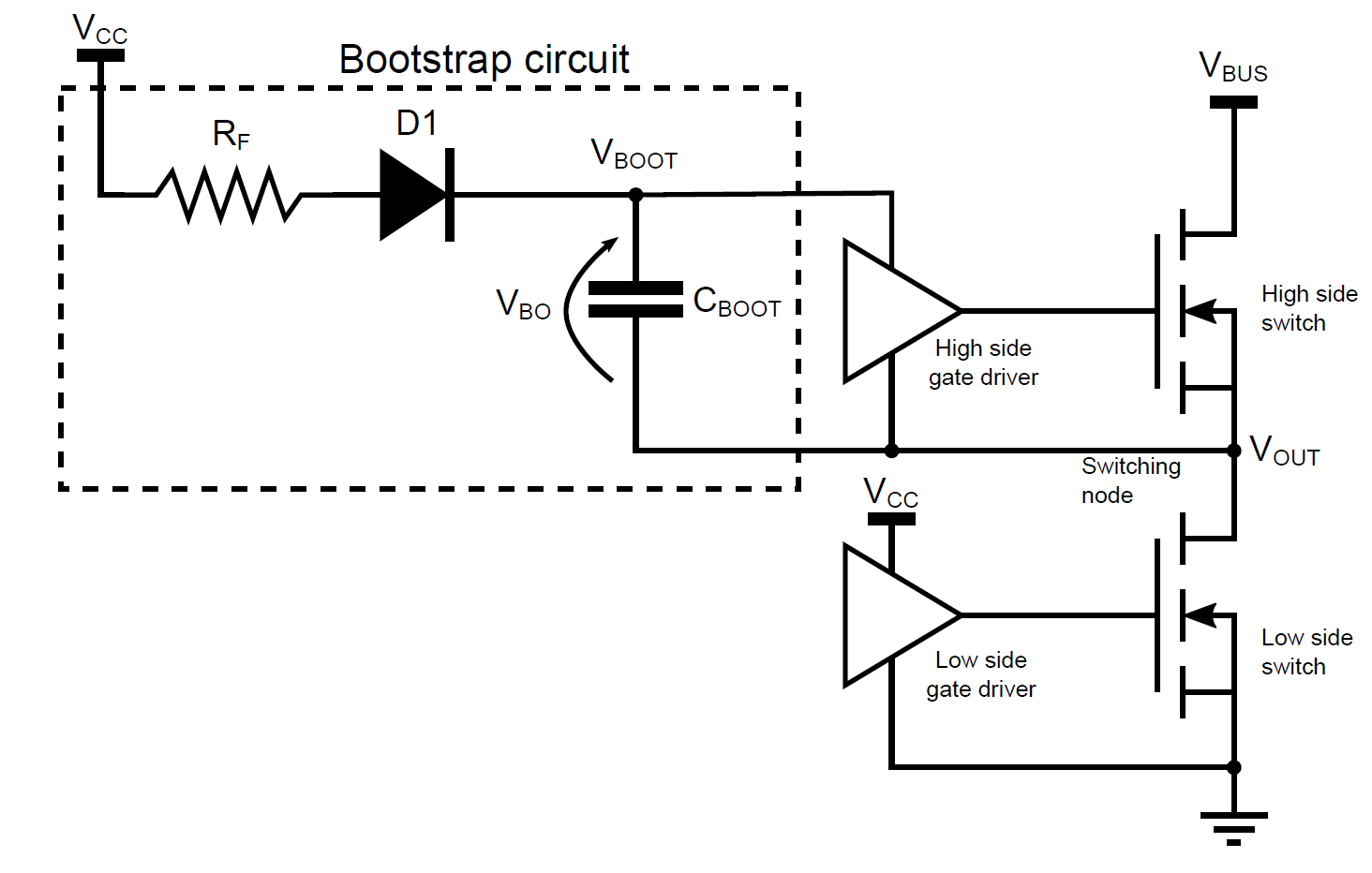
All pins except BOOT have been analyzed before. This pin manages to solve a critical problem: when the high-side MOSFET turns on, the input voltage flows to its source terminal, making the source voltage approach the input voltage. Hence, to keep the high-side MOSFET fully enhanced, the gate must be applied a voltage greater than
When the high-side MOSFET turns off and the low-side MOSFET turns on, the lower terminal of
The reason why PMOS is not used here is that PMOS occupies larger area under the same performace because the mobility of electrons is twice or three times than holes.
4. Low Dropout Regulator (LDO)
LDO is another type of power management circuit, only applicable in decreasing the voltage. LDO can be regarded as a variable resistance with a feedback loop. It uses an error amplifier and an NMOS to perform this function.
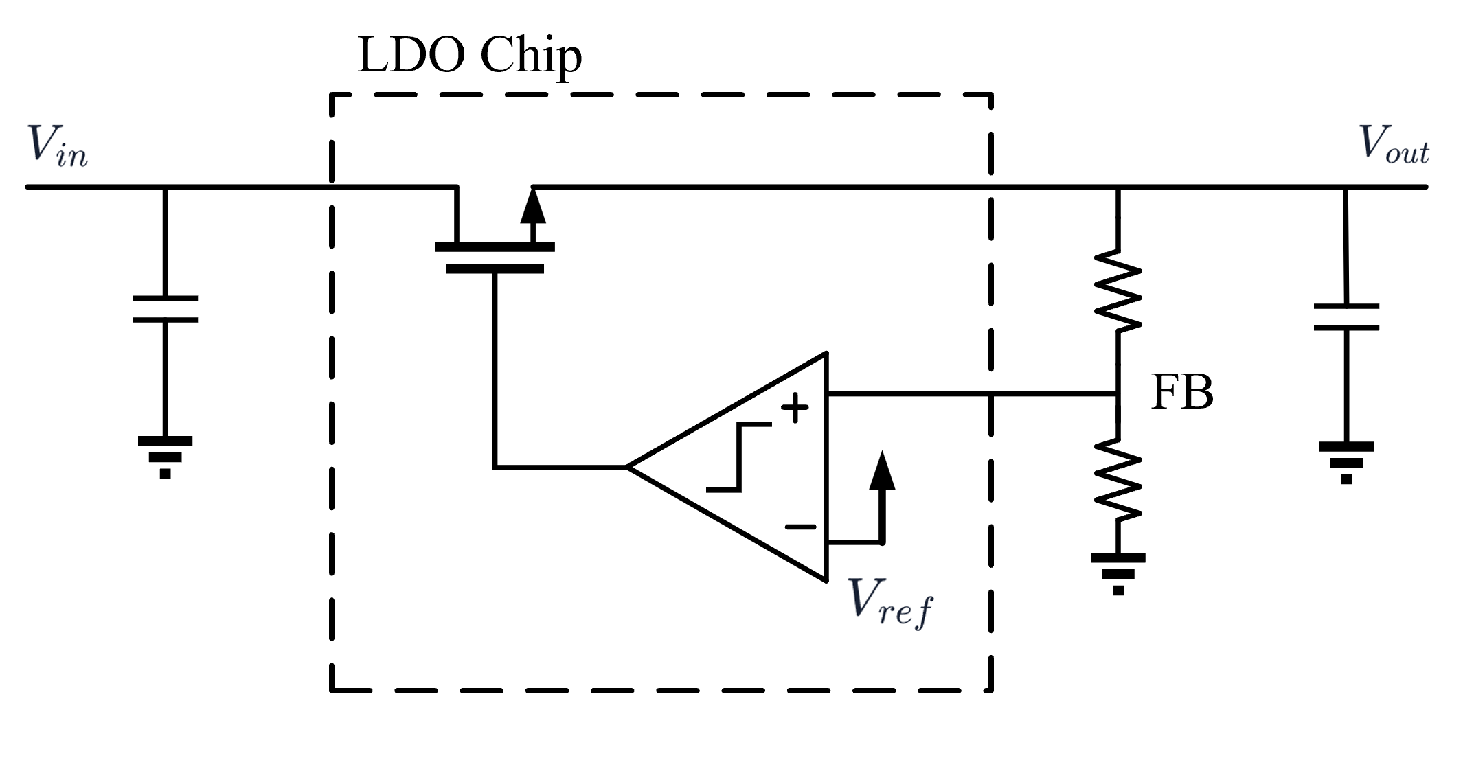
LDO has no switching inside the chip, so there is almost no switching ripple. Instead, the regulation is implemented by a continuous negative feedback loop. Inside the chip, an error amplifier continuously monitors the scaling output voltage from the feedback resistors and compares it with an internal reference voltage. If the feedback voltage slightly exceeds the reference, the error amplifier seamlessly adjusts the gate voltage of the power MOSFET (such as an NMOS pass element), smoothly increasing its equivalent channel resistance. This continuous adjustment increases the voltage drop across the MOSFET, immediately pulling the output voltage back down to the target value. Through this analog linear feedback process, the output voltage is perfectly stabilized without introducing high-frequency switching noise. Since the feedback resistors are typically placed outside the chip, we can select their values to configure the desired output voltage.
We denote the resistor between FB and
Reverse the equation,
Note that the MOSFET on the main power path requires a minimum voltage headroom to remain in its active conductive region, which determines the minimum input-to-output voltage difference known as the dropout voltage. You can find this critical parameter in the datasheet.
One inherent drawback of LDOs is their low efficiency under large voltage gaps. Inside the chip, the dominant energy loss does not stem from the quiescent current of the control circuitry, but rather from the power dissipation across the internal pass MOSFET itself. Since the full load current passes through this transistor, it drops the excess voltage (
Since the feedback current and internal quiescent current are small enough to be neglected, the input current is practically identical to the output current. Thus, the efficiency of an LDO is tightly bounded by the voltage ratio:
The rest of the electrical energy is entirely dissipated as heat within the package. Therefore, LDOs are not suitable for applications with a large dropout voltage combined with high load currents, as the excessive thermal stress can rapidly overheat the device.
Despite the efficiency penalty, LDOs outperform buck converters in nearly all other performance metrics, offering ultra-low output ripple, zero switching EMI, and excellent transient response. Consequently, in practical power system designs, they are frequently combined to achieve both high efficiency and high purity. For instance, if the system requires a clean, low-noise 12V supply from a lower input power source, a boost converter is first applied to efficiently raise the voltage to around 13V or 14V. Then, an LDO is cascaded to drop and precisely stabilize the voltage to 12V. This architecture allows the LDO to effectively reject the high-frequency switching ripple inherited from the boost converter, providing an exceptionally quiet and high-quality power rail for sensitive analog circuits.
Reference
[1] B. Razavi, “The Design of An LDO Regulator,” IEEE Solid-State Circuits Magazine, vol. 14, no. 2, pp. 7-11, Spring 2022, doi: 10.1109/MSSC.2022.3164746.
[2] TPS54302 4.5V to 28V Input, 3A Output, EMI-Friendly Synchronous Step-Down Converter Datasheet, Texas Instruments Incorporated, Doc. No. SLVSDG6C, May 2016, Revised March 2026.
[3] “Considerations on bootstrap circuitry for gate drivers,” STMicroelectronics, Geneva, Switzerland, Application Note AN5789, Rev. 1, Mar. 2022.